In advanced semiconductor sub-7nm fab nodes, micro-contamination from vessel inner walls can drastically degrade yield rates. Achieving a surface roughness of Ra ≤ 0.25μm via specialized Electropolishing (EP) is mandatory for housing 6N/7N electronic specialty gases (ESGs) and high-purity chemical precursors.
Key Takeaways for Fab Engineers & Procurement Directors
- Surface Roughness Standard: Achieving Ra ≤ 0.25μm (10 μin) removes microscopic pits, preventing gas moisture entrapment and particle generation[cite: 1].
- Passivation & Chromium Oxide Layer: EP enriches the Chromium-to-Iron (Cr/Fe ≥ 1.5) ratio on the inner wall, forming a dense passive film against corrosive fluorine and chlorine gases.
- Premium Material Selection: Utilizing 316L VIM-VAR (Vacuum Induction Melting / Vacuum Arc Remelting) stainless steel eliminates non-metallic inclusions prior to polishing.
- Class 10/100 Cleanroom Processing: Final DI water rinsing, helium leak auditing, and ultra-pure nitrogen purging must occur inside certified cleanroom environments.
Why Inner Surface Finish Matters in UHP Chemical Containment
Electronic Specialty Gases (ESGs) such as Silane (SiH4), Nitrogen Trifluoride (NF3), and Hydrogen Chloride (HCl) require extreme purity levels (99.9999% to 99.99999%). Conventional mechanical grinding leaves micro-scratches and embedded abrasive particles on vessel walls. Under high pressures, these surface defects become active sites for particle outgassing, trace moisture absorption, and severe pitting corrosion[cite: 1].
The Electropolishing (EP) Electrochemical Reaction
Electropolishing is an electrochemical process that selectively dissolves the microscopic high-points (peaks) on a metal surface faster than the low-points (valleys). When 316L stainless steel vessels are submerged in an anodic acid electrolyte bath with controlled current density, the surface micro-profile is leveled down to an ultra-smooth mirror finish (Ra ≤ 0.25μm)[cite: 1].
Mechanical Polishing vs. High-Grade Electropolishing (EP)
| Quality Parameter | Mechanical Polishing (MP) | Ultra-Pure Electropolishing (EP) |
|---|---|---|
| Surface Roughness (Ra) | Ra 0.4μm – 0.8μm | Ra ≤ 0.25μm (10 μin) Mirror Finish[cite: 1] |
| Passive Oxide Layer | Disrupted mechanically | Dense Cr2O3 layer (Cr/Fe ratio ≥ 1.5) |
| Outgassing & Particle Trapping | High moisture retention | Ultra-low outgassing & zero particle shed |
| Target Applications | Industrial & General Chemical | 6N/7N Semiconductor Gases & Photolithography[cite: 1] |
Quality Verification & Cleanroom Testing Protocols
1. Scanning Electron Microscopy (SEM) & Auger Analysis (AES)
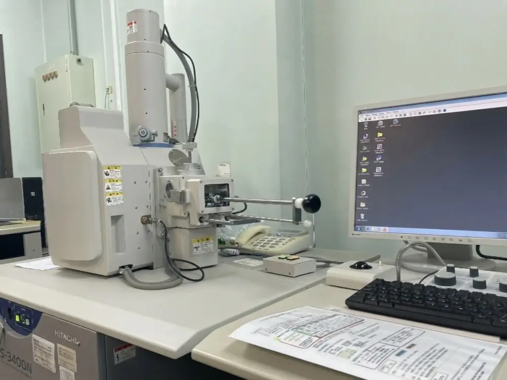
To guarantee that no micro-fissures remain, finished vessel walls undergo SEM metallurgical inspection at 10,000x magnification. Auger Electron Spectroscopy (AES) measures oxide depth profile to ensure a uniform passivation thickness exceeding 25 Ångströms.
2. Helium Mass Spectrometer Leak Detection
Ultrasensitive containment integrity is verified using vacuum-chamber helium mass spectrometer leak detectors. Ultra-pure semiconductor cylinders must achieve a certified leak rate below 1 × 10⁻⁹ mbar·L/s[cite: 2].
Keystone Vessel: Semiconductor-Grade Containment Excellence
Equipped with state-of-the-art electropolishing lines and Class 10/100 cleanroom packaging, Keystone Vessel delivers ASME & DOT certified UHP gas cylinders and chemical pressure vessels for global semiconductor foundries.
Download UHP Technical Specification Direct WhatsApp Semiconductor Engineering Contact (+86 186 7228 4442)
Frequently Asked Questions (FAQ)
Q1: What does Ra ≤ 0.25μm signify in ultra-pure pressure vessels?
Ra (Roughness Average) ≤ 0.25μm (or 10 micro-inches) indicates an ultra-smooth, mirror-like inner surface finish that prevents sub-micron particle accumulation and gas contamination in semiconductor manufacturing[cite: 1].
Q2: Why is 316L VIM-VAR stainless steel preferred for electropolishing?
Vacuum Induction Melting followed by Vacuum Arc Remelting (VIM-VAR) yields ultra-clean steel with minimal manganese sulfide inclusions, preventing pitting defects during anodic electropolishing.